A Second-Order Purely VCO-Based CT ΔΣ ADC Using a Modified DPLL Structure in 40-nm CMOS
摘要
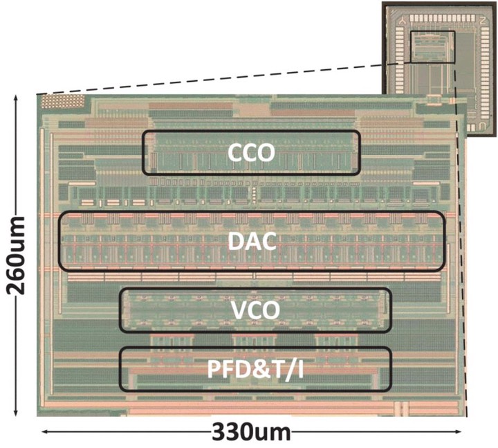
This article presents a power-efficient purely voltage-controlled oscillator (VCO)-based second-order continuous-time (CT) ΔΣ analog-to-digital converter (ADC), featuring a modified digital phase-locked loop (DPLL) structure. The proposed ADC combines a VCO with a switched-ring oscillator (SRO)-based time-to-digital converter (TDC), which enables second-order noise shaping without any operational transconductance amplifiers (OTAs). The nonlinearity of the front-end VCO is mitigated by putting it inside a closed loop. An array of phase/frequency detectors (PFDs) is used to relax the requirement on the VCO center frequency and thus reduces the VCO power and noise. The proposed architecture also realizes an intrinsic tri-level data-weighted averaging (DWA). A prototype chip is fabricated in a 40-nm CMOS process. The proposed ADC achieves a peak signal-to-noise-and-distortion ratio (SNDR) of 69.4 dB over 5.2-MHz bandwidth, while operating at the 260 MS/s and consuming 0.86 mW from a 1.1-V supply.